Report on One - Day Workshop on PCB Design
Department of Electronics and Communication Engineering organized a One - Day Workshop on PCB Design” under CoE in Robotics and Industrial Automation. In this training, students got to know about single layer PCB Design using CADENCE-Allegro. This training was conducted and coordinated by Mr. L. David William Raj, Assistant Professor, Department of Electronics and Communication Engineering. 42 students from ECE, CSE, IoT, Aeronautical and Aerospace Enginering from 1st and 2nd Year participated in this workshop.
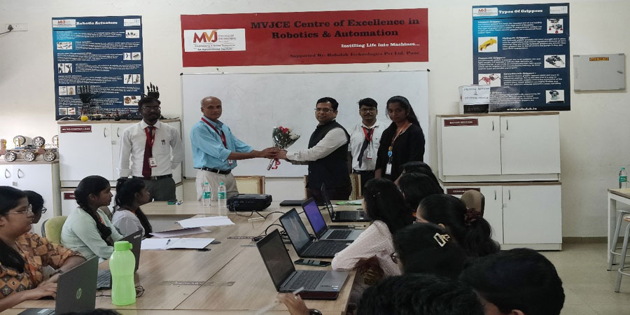 Dr. Remashan Kariyadan presented the flower bouquet to the guest Mr. Amit Goel, Scientist, LRDE, DRDO.
 The program started on 18th July 2023 at 09.30 AM in Robotics and Industrial Automation Lab. The dignitaries on the stage were Dr. Remashan Kariyadan, Professor,Department of Industrial IoT, MVJCE, Mr. Amit Goel, Scientist, LRDE, DRDO. Dr. Remashan Kariyadan, Professor,Department of Industrial IoT welcomed the guest and presented the flower bouquet to the guest Mr. Amit Goel, Scientist, LRDE, DRDO.
Session-1 (18.07.2023)
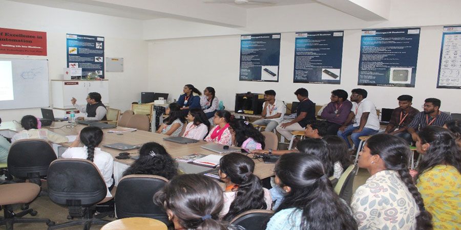
The first session started off with the lecture of Mr. Amit Goel, Scientist, LRDE at 10 AM. His talk was based on the basics of PCB fundamentals.
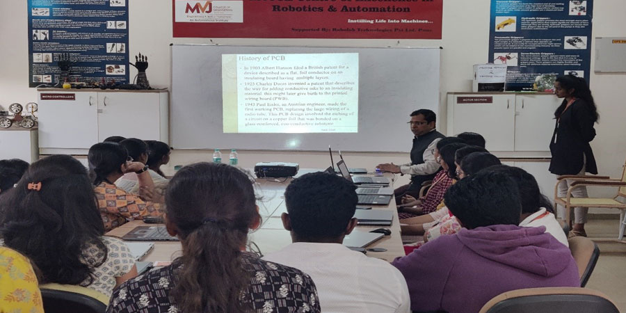 Session on History of PCB given by Mr. Amit Goel, Scientist, LRDE, DRDO.
 Session-2 (18.07.2023)
The second session started with the lecture of Mr. Amit Goel, Scientist, LRDE and his team member. In this session, they discussed the procedure of PCB designing in CADENCE-Allegro step by step.
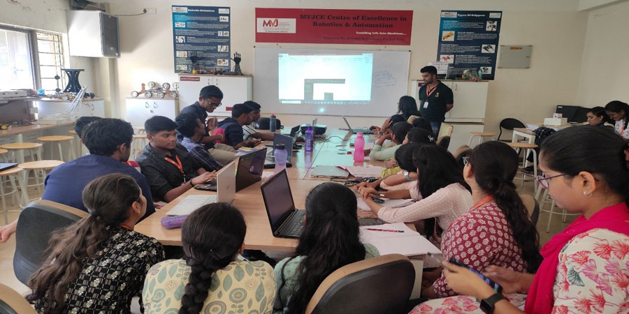 Hands on Session on Gerber file generation using cadence Allegro.
Outcomes:
- Students learnt about the basics of PCB Design.
- Students learnt about the identification of Footprints using Cadence Allegro.
- Students learnt about design rules to be followed while designing any circuit and how to place components in PCB.
Other Events