The AICTE-sponsored ATAL Faculty Development Programme on Recent Developments in High-Speed Semiconductor Devices and Next Generation Flexible and Transparent Devices: Changing the Semiconductor World was organized by the Department of Electronics and Communication Engineering from October 16th to 21st, 2023, in Seminar Hall 4, running from 9:30 am to 5:00 pm.
The event was presided over by Principal Dr. V. Suresh Babu, Vice-Principal Dr. M. Brindha, and the coordinator, Professor Dr. Remashan Kariyadan. The resource persons for the program were:
- Dr. K. N. Bhat, Former Professor, IIT Madras & IISc, Bangalore.
- Mr. Chandrasekhar Kypa, Associate Vice President, Quest Global, Bangalore.
- Dr. V. Suresh Babu, Principal, MVJ College of Engineering, Bangalore.
- Mr. Satya Marni, R&D Director, Synopsys, Bangalore.
- Dr. Navakanta Bhat, Professor, IISc, Bangalore.
- Dr. Sivaprasad Kotamraju, Associate Professor, IIIT Sri City, Chittoor.
- Dr. S. Sundar Kumar Iyer, Professor, IIT Kanpur.
Inauguration Session:
The FDP was inaugurated by Dr. K. N. Bhat, Former Professor, IIT Madras & IISc, Bangalore, on October 16th, 2023, at 10:00 am with the lamp lighting. The Principal, Dr. V. Suresh Babu of the institute, addressed the participants and congratulated them for registering for this FDP. A total of 35 faculty members from various technical institutions were registered and participated in the faculty development program.Day 1: Semiconductor Devices – Dr. K N Bhat (16.10.23 – FN)
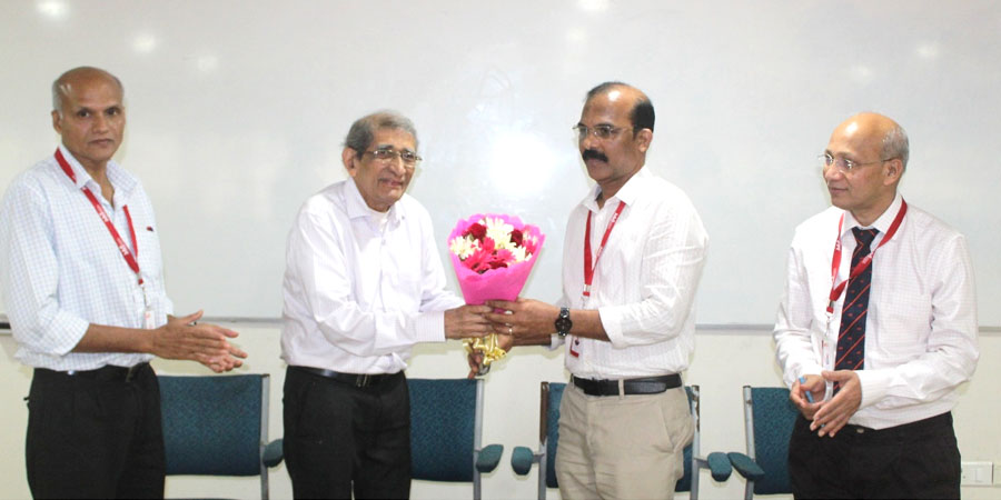
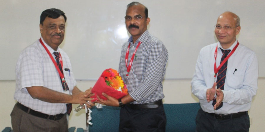
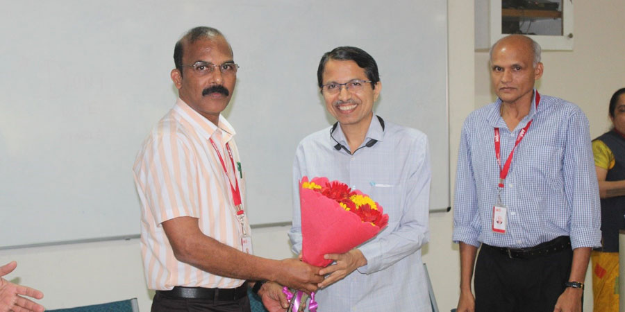
Dr. Suresh Babu.V, Principal, MVJ College of Engineering, Bangalore welcoming the chief guest Dr. K N Bhat, Former Professor, IIT Madras & IISc, Bangalore with a bouquet.
Dr. K. N. Bhat started his presentation with the emphasis on the importance of understanding the operation of a p-n junction diode. First, Dr. Bhat explained the mechanisms responsible for current flow in a semiconducting material, namely diffusion and drift. Next, he explained the operation of p-n junction diode, BJT and MOSFET.
Prof Bhat also highlighted the advantage of GaAs material in comparison with silicon material and why MOS technology is not available in the case of GaAs material. Also, design approach of high voltage of devices based on SI was discussed.
Day 1: Semiconductor Devices – Dr. K N Bhat (16.10.23 – AN)
In the afternoon session, Prof. Bhat presented theory, technology, and applications of MEMD-based pressure sensors.
Prof Bhat explained how pressure sensors can be used to monitor BP of a human being (patient). Also, the type of pressure sensors used in aircraft to monitor the altitude of the aircrafts and the depth monitoring sensor for marine engineering was discussed.
He discussed the different types of pressure sensors like Piezoelectric Pressure sensor, Capacitive Pressure sensor and Piezoresistive Pressure sensor. Also, he explained the fabrication of these pressure sensors
End of day 1 session with the resource person Dr. K N Bhat.
Day 2: High Speed Semiconductor Devices – Mr. Chandrasekhar Kypa, (17.10.23 – FN)
Mr. Chandrasekhar Kypa highlighted how speed of Si-based devices can be enhanced by reducing the technology node down to 3 nm and mentioned that silicon-based devices now constitute approximately 95% of all semiconductor devices sold worldwide. Also, he discussed the structure of a 3nm FinFET.
On the other hand, the speaker brought out a very important concept that for ultrahigh-speed applications the III–V semiconductors have advantages over silicon because of their higher carrier mobilities and higher effective carrier velocities. The most important compound semiconductors for high-speed devices are, GaAs / AlGaAs, InP / InGaAs, InP / InGaAsSb, and GaAs / InGaP.
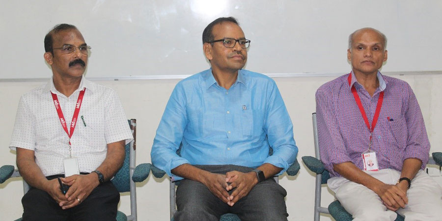
(L to R) Dr.Suresh Babu.V, Principal, MVJ College of Engineering, Bangalore, the chief guest Mr. Chandrasekhar Kypa, Associate Vice President, Quest Global, Bangalore, Dr.Remashan, Professor, Dept. of ECE on the Dias.
Day 2 High Speed Semiconductor Devices – Mr. Chandrasekhar Kypa, (17.10.23 – FN)
Mr. Kypa, in the afternoon session, introduced AI chips- the chips specific to AI applications. He described different types of AI chips. (i) universal chips that can support AI applications efficiently through hardware and software optimization, such as GPU; (ii) chips that focus on Accelerating Machine Learning (especially neural networks and deep learning), which is the most popular form of AI chips at present. (iii) Neuromorphic computing chips inspired by biological brain.
To realize these kinds of chips, we need to have CMOS technology that can realize the following:
- On Chip Memory (Synaptic Array): Distributed SRAM, ReRAM, PCRAM, etc.,
- CMOS Process: Process Node (16, 7, 5 nm), CMOS 3D Stacking: 2.5D IC / SiP, 3D-stack Technology, Monolithic 3D, etc.,
- New Technologies: 3D NAND, Flash Tunnelling FETs, FeFET, FinFET.
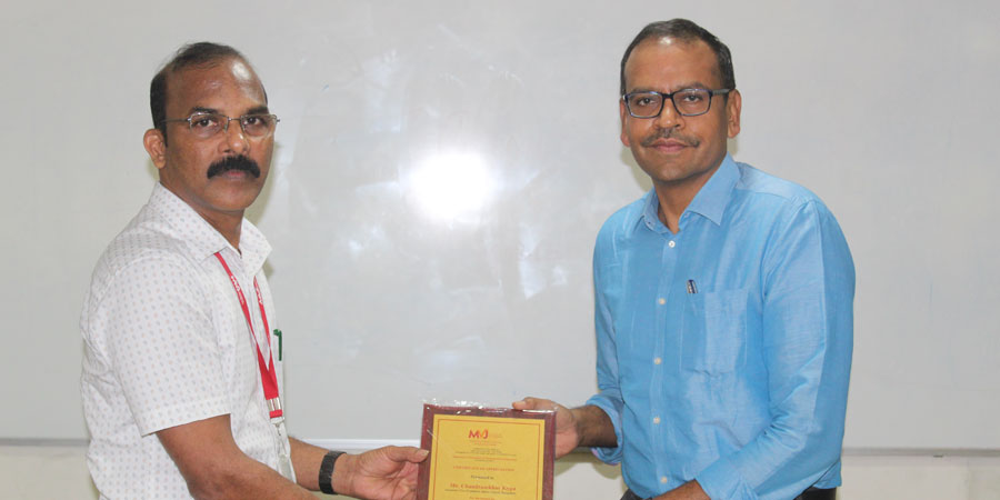
Dr.Suresh Babu.V, Principal, MVJ College of Engineering, Bangalore honoring the chief guest Mr. Chandrasekhar Kypa, Associate Vice President, Quest Global, Bangalore, with a memento.
Day 3: Organic Electronic Devices – Dr. V Suresh Babu -18.10.23 (FN)
Dr Suresh Babu started the session with the fundamentals of semiconductors particularly silicon materials. He then brought out the major drawback of silicon semiconductor and how this drawback can be overcome by bringing in a new material called ‘organic semiconductor”.
He then mentioned important applications of organic materials such as Organic light-emitting diodes, Organic solar cell, Thin-film transistors, Biosensors and Memory devices.
Among the above applications, Dr Suresh Babu picked up one application, i.e., thin-film transistors and discussed 4 types of device structures available to fabricate Organic TFTs. He also explained the basic processing steps involved in the organic TFT fabrication.
Dr. Shrinivas L Gombi, Dean of Academics, MVJ College of Engineering, Bangalore welcoming the chief guest Dr.Suresh Babu.V, Principal, MVJ College of Engineering, with a bouquet.
Day 3: Organic Electronic Devices – Mr. Satya Marni – 18.10.23 (AN)
Mr. Satya Marni started the session with Organic TFTs and its potential applications in OLEDs and in sensors.
He highlighted the merits and demerits of each one of the 4 typical device structures available to fabricate TFTs. These are bottom-gate top contact, bottom-gate bottom contact, top-gate bottom contact and top-gate top contact.
Mr. Satya Marni delivering his interesting lecture during the afternoon session
He explained the processing steps involved in the fabrication of solution processed organic TFTs using top gate and bottom contact device structure. The organic semiconductor and the organic gate dielectric used were TIPS-pentacene and CYTOP, respectively. Mr Satya also pointed out the major hurdles in the development of organic TFTs.
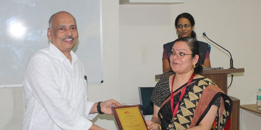
Dr. Brindha. M, Vice-Principal, MVJ College of Engineering, Bangalore, honoring the chief guest Mr. Satya Marni, R&D Director, Synopsys, Bangalore with a memento.
Day 4: Nano Electronic Devices – Dr. V Suresh Babu -19.10.23 (FN)
Dr. Suresh Babu started the session with looking at the technology node from 10 microns down to 3 nm and a question was addressed to the participants: Is the change in the technology node in line with the MOORE’s Law predicted in 1965? He pointed out some of the issues involved in the scaling of MSFETs, such as supply voltage, threshold voltage, gate oxide thickness, substrate doping etc.
He also touched up on the properties of nanomaterials and its application in various fields such as Paints, Sunscreens and Cosmetics, Effluent treatment, Medicine, Gas Sensors, Food, Construction and Energy.
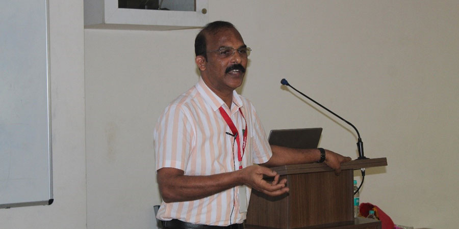
Dr. Suresh Babu V, Principal, MVJ college of Engineering, Bangalore delivering his interesting lecture during the forenoon session
Day 4: Nano Electronic Devices – Dr. Navakanta Bhat – 19.10.23 (AN)
Dr. Navakanta Bhat started the session on the Nano electronic devices by emphasizing scaling of MOS devices and how these scaling affects the device and circuit performance parameters. He also described how the semiconductor devices impacted human life.
The speaker also emphasized different mechanism that can happen in nano-MOSFETs. These are gate tunnelling, channel quantization and quasi ballistic transport.
The speaker also examined whether graphene can be used for realizing CMOS technology? and concluded that graphene transistor is a very bad switch.
He also looked at a couple of novel transistors such as MoS2 Steep Slope Transistors, and FETs with Programmable Transport between Thermionic and Tunnelling. He then concluded that careful optimization of Material, Process and Device Design is required to tap the potential of the novel transistors.
Dr. Suresh Babu. V, Principal, MVJ College of Engineering, Bangalore welcoming the chief guest Dr. K N Bhat, Former Professor, IIT Madras & IISc, Bangalore with a bouquet
Dr. K N Bhat delivering his lecture during the forenoon session
Day 5: Transparent Electronic Devices- Dr. Sivaprasad Kotamraju – 20.10.23 (FN)
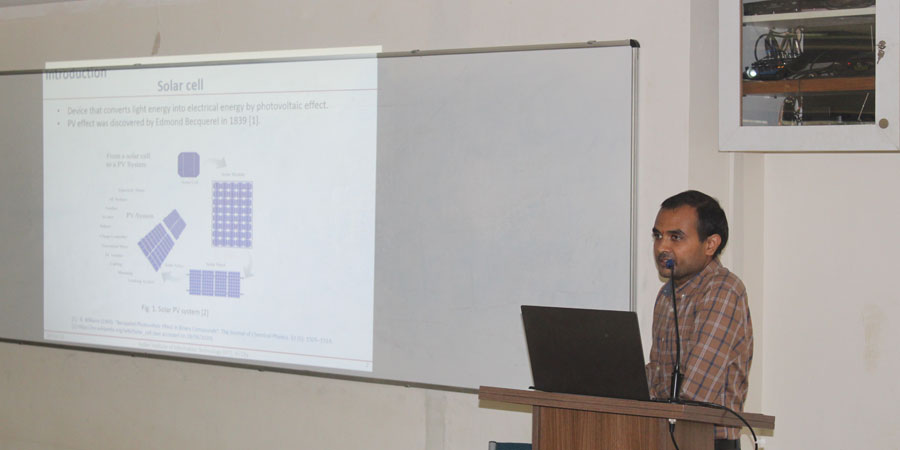
Dr. Sivaprasad Kotamraju explained the single-junction solar cell, multi junction solar cells and III-V solar cells.
The speaker underlined transparent solar cells that could turn windows into power generators. Solar windows look like regular glass windows, but act like solar panels, generating electricity from the sun. These transparent solar cells absorb only infrared and ultraviolet light. Visible light passes through the cells unimpeded, so our eyes do not know there are there.
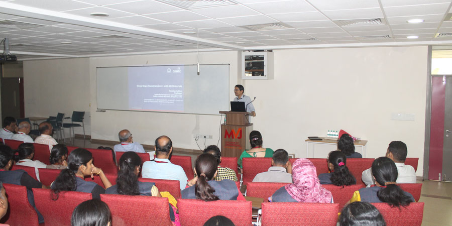
Dr. Sivaprasad Kotamraju delivering his lecture during the forenoon session
Day 5: Industrial Visit – Semiconductor Technology & Applied Research Centre (STARC), DRDO, Bangalore – 20.10.23 (AN)
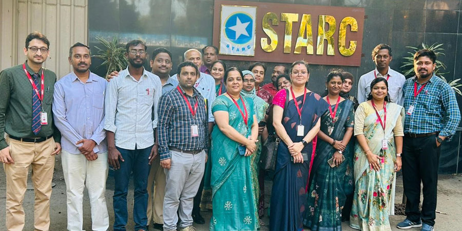
In the afternoon session, the participants visited Semiconductor Technology & Applied Research Centre (STARC) – DRDO, Bangalore which has the following facilities – MEMS Fabrication, MEMS Packaging & Testing, and 1-micron digital CMOS IC fabrication.
Industrial visit to Semiconductor Technology & Applied Research Centre (STARC), DRDO, Bangalore.
Day 6: Flexible Electronic Devices, Dr. S Sundar Kumar Iyer – 21.10.23 (FN)
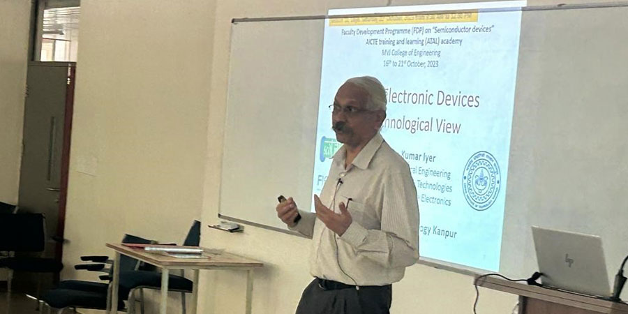
Dr. Sunder Kumar Iyer started the presentation explaining the drawbacks of conventional electronics and then moved on to the motivation for flexible electronic devices. He also explained how a material can be made flexible and what are the challenges facing the development of flexible electronic devices.
The speaker then highlighted the advantages of flexible organic materials and then described various organic devices and its applications areas – Packaging and Labels, Health Care, Strategic Sectors, Wearables, Consumer Electronics and Automobile.
At the end of the session, the speaker provided a couple of “Take Home Message” in connection with organic flexible devices
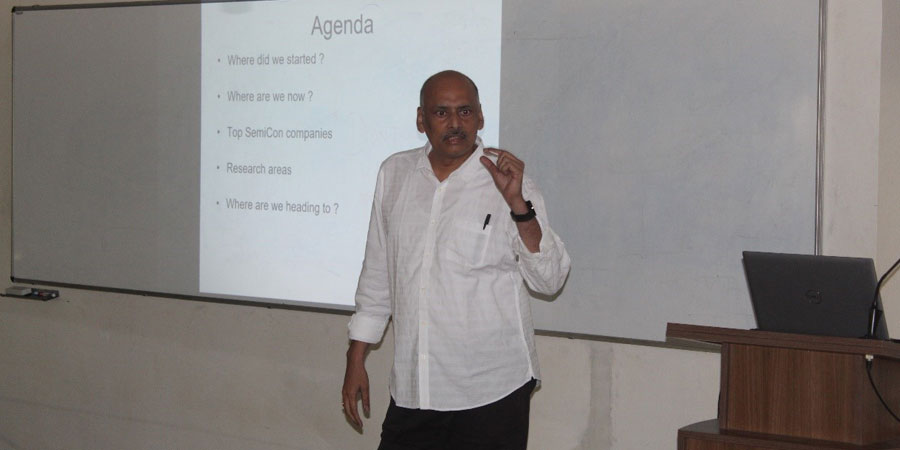
Dr Sunder Kumar Iyer delivering his lecture during the forenoon session
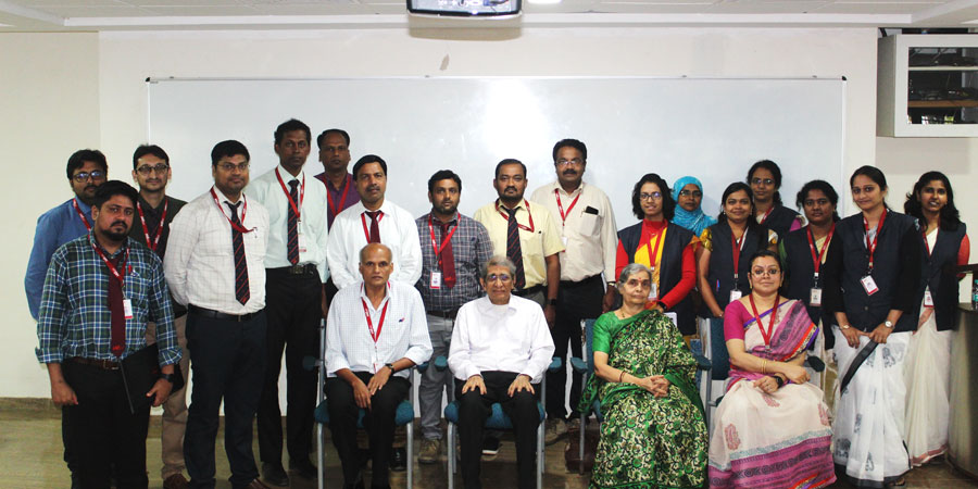
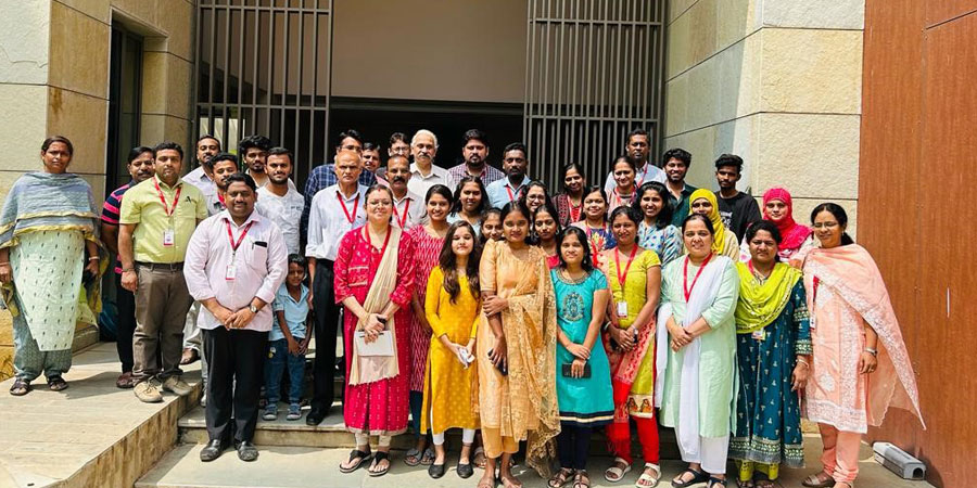
Photo session with the chief guest Dr Sunder Kumar Iyer on the last day of the FDP
Continuous Comprehensive Assessment:
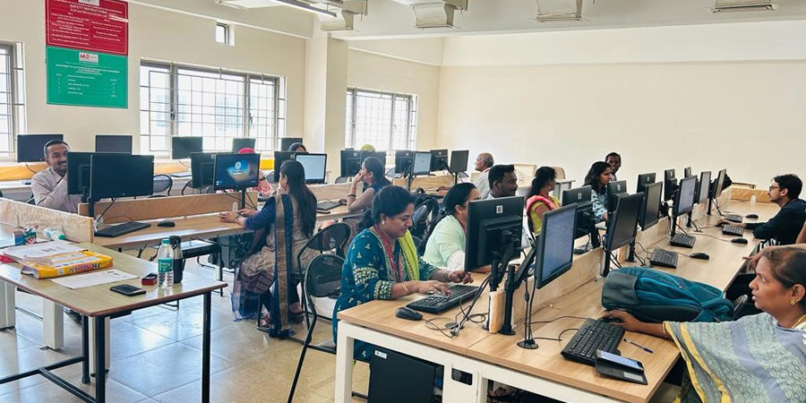
After the completion of FDP, participants took part in the continuous comprehensive assessment and given the feedback.
Participants undertaking the comprehensive assessment on the last day of the session
Conclusion:
In the conclusion, the six – day ATAL Academy Sponsored FDP laid the platform for the participants to carry out future research activities in their field of interest. The active involvement of the participants in this FDP reflected their eagerness to learn latest developments happening in the semiconductor field.
Outcome of the FDP:
Overall, 35 faculty members from different colleges have actively participated in the ATAL FDP. This FDP was a good learning experience for the all the participants. They had the opportunity to interact with the resource persons and discuss their published research articles. They had lab sessions which were indeed helpful to their research work.
