Department of Electronics and Communication Engineering organized a club activity “PCB DESIGN CHALLENGE COMPETITION” under CoE in Robotics and Industrial Automation. InPCB Design challenge competition, students had to create Schematic Design, PCB Layout and Extract the Gerber file corresponding to the given circuit challenge. It was conducted and coordinated by Mr. L. David William Raj (AP/ECE) and Dr.Utsab Banerjee (AP/ECE). There were 30 participantsfrom different streamsof 2nd, 4th Semester.
The program started on 22nd July 2023 at 01.00 PM. Prof. Murali C, Former Vice President, IETE, New Delhi was the guest for the programme.
The Competiton started with an introduction of the Chief guest. Prof.C Murali, Former Vice President, IETE, New Delhi,explained the basic rules and regulations, followed by providing the details of the circuit to be designed.
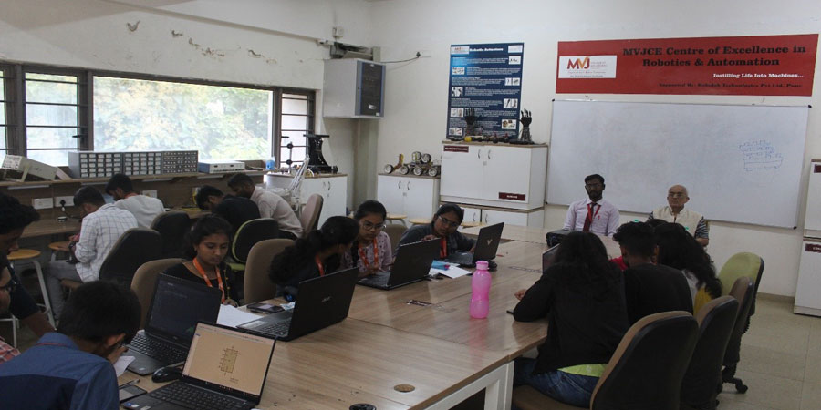
Participants preparing the schematic designs under the close supervision of Prof. C. Murali, Former Vice President, IETE, New Delhi.
The competition started with the students creating the schematic PCB Design of the given circuits.The students participating in the competition came with Pre installed EDA tools like Cadence Allegro/ Eagle CAD/ Tinker CAD/ Multisim/ Proteus.
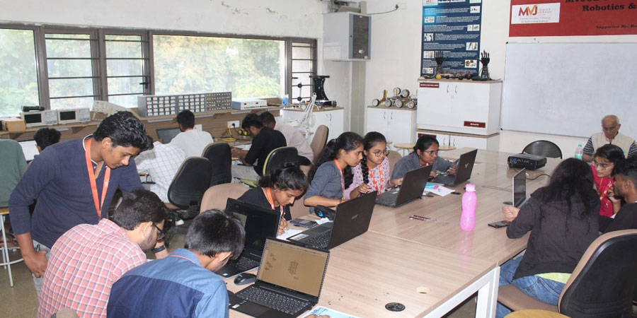
Participants busy in preparing layout
The single Layer PCB Schematic design was validated by the chief guest. After Validation the students were instructed to extract the Gerber file for their design schematics. The students got an opportunity to apply their technical knowledge in creating practical desings.
Runners of the PCB Design Challenge competition organized by Robo Lab on 22.07.2023
In addition to the Winners, certificates were issued to all the registered participants.
Winners
- Ashish Ramesh (1MJ22CS021)
- Jonathan Daniel (1MJ22IO008)
Runners
- Karthik Gururaj Badami (1MJ21EC054)
- Avala Ganesh Yadav (1MJ21EC012)
Outcomes:
- Students designed the circuit using Cadence Allegro/ Eagle CAD/ Tinker CAD.
- Students extracted the Gerber file for their schematic design.
- Students gained valuable experience in designing and extracting electrical circuits.


